Renesas Electronics 5V2310PGGI High Performance Clock Buffer 24-Pin TSSOP
- RS Stock No.:
- 254-4947P
- Mfr. Part No.:
- 5V2310PGGI
- Manufacturer:
- Renesas Electronics

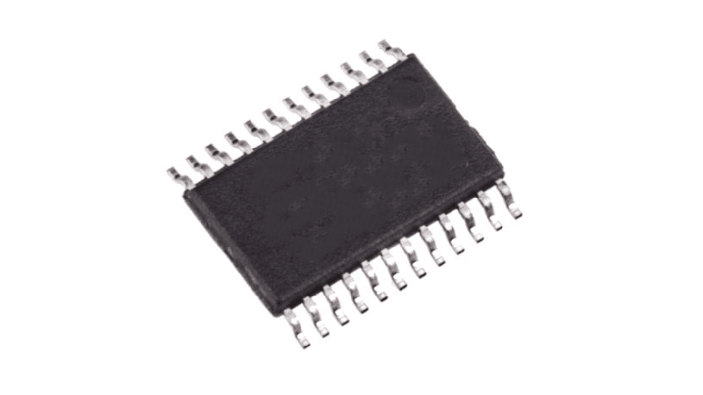
The image is for reference only, please refer to product details and specifications
Bulk discount available
Subtotal 10 units (supplied in a tube)*
TWD1,335.00
(exc. GST)
TWD1,401.80
(inc. GST)
Add 10 units to get free delivery
Last RS stock
- Final 186 unit(s), ready to ship from another location
Units | Per unit |
|---|---|
| 10 - 18 | TWD133.50 |
| 20 - 24 | TWD131.50 |
| 26 - 98 | TWD127.00 |
| 100 + | TWD110.00 |
*price indicative
- RS Stock No.:
- 254-4947P
- Mfr. Part No.:
- 5V2310PGGI
- Manufacturer:
- Renesas Electronics
Specifications
Product overview and Technical data sheets
Legislation and Compliance
Product Details
Find similar products by selecting one or more attributes.
Select all | Attribute | Value |
|---|---|---|
| Brand | Renesas Electronics | |
| Product Type | High Performance Clock Buffer | |
| Maximum Input Frequency | 200MHz | |
| Mount Type | Surface | |
| Maximum Propagation Delay Time | 2.8ns | |
| Package Type | TSSOP | |
| Pin Count | 24 | |
| Number of Outputs | 10 | |
| Minimum Supply Voltage | 2.3V | |
| Maximum Supply Voltage | 3.6V | |
| Minimum Operating Temperature | -40°C | |
| Maximum Operating Temperature | 85°C | |
| Standards/Approvals | RoHS | |
| Series | IDT5V2310 | |
| Automotive Standard | No | |
| Select all | ||
|---|---|---|
Brand Renesas Electronics | ||
Product Type High Performance Clock Buffer | ||
Maximum Input Frequency 200MHz | ||
Mount Type Surface | ||
Maximum Propagation Delay Time 2.8ns | ||
Package Type TSSOP | ||
Pin Count 24 | ||
Number of Outputs 10 | ||
Minimum Supply Voltage 2.3V | ||
Maximum Supply Voltage 3.6V | ||
Minimum Operating Temperature -40°C | ||
Maximum Operating Temperature 85°C | ||
Standards/Approvals RoHS | ||
Series IDT5V2310 | ||
Automotive Standard No | ||
The Renesas Electronics high performance, low skew clock buffer that operates up to 200MHz. Two banks of five outputs each provide low skew copies of CLK. Through the use of control pins 1G and 2G, the outputs of banks 1Y(0:4) and 2Y(0:4) can be placed in a low state regardless of CLK input. The device operates in 2.5V and 3.3V environments. The built-in output enable glitch suppression ensures a synchronized output enable sequence to distribute full period clock signals. The IDT5V2310 is characterized for operation from -40°C to +85°C.
High performance 1:10 clock driver for general purpose applications
Pin-to-pin skew < 100 ps
VDD range is 2.3 V to 3.6 V
Output enable glitch suppression
Distributes one clock input to two banks of five outputs
25 Ω on-chip series dampening resistors
Available in TSSOP package