Renesas Electronics 5PB1216NDGK Clock Buffer 20-Pin VFQFPN
- RS Stock No.:
- 262-8966
- Mfr. Part No.:
- 5PB1216NDGK
- Manufacturer:
- Renesas Electronics

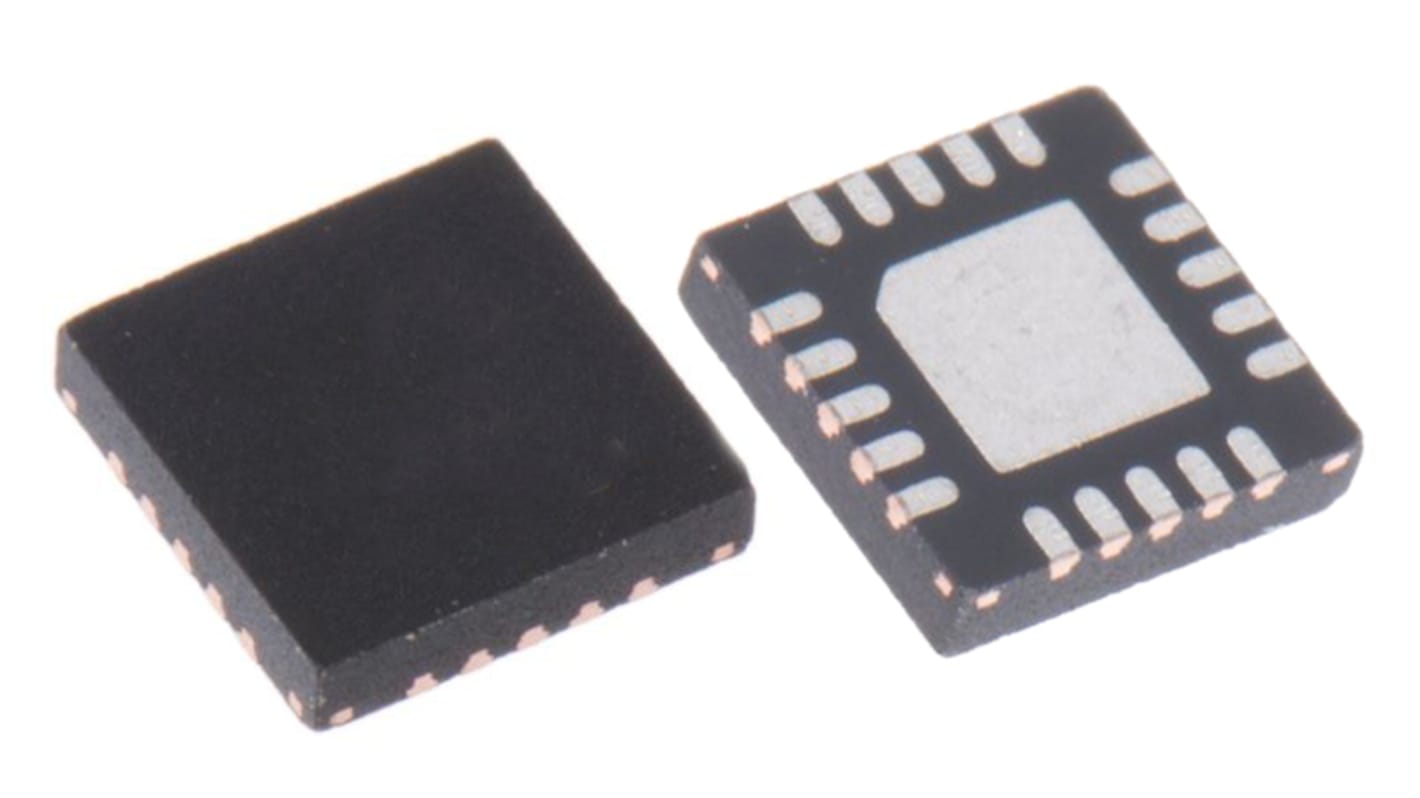
The image is for reference only, please refer to product details and specifications
Currently unavailable
We don't know if this item will be back in stock, RS intend to remove it from our range soon.
- RS Stock No.:
- 262-8966
- Mfr. Part No.:
- 5PB1216NDGK
- Manufacturer:
- Renesas Electronics
Specifications
Product overview and Technical data sheets
Legislation and Compliance
Product Details
Find similar products by selecting one or more attributes.
Select all | Attribute | Value |
|---|---|---|
| Brand | Renesas Electronics | |
| Product Type | Clock Buffer | |
| Maximum Input Frequency | 200MHz | |
| Maximum Propagation Delay Time | 2.7ns | |
| Package Type | VFQFPN | |
| Pin Count | 20 | |
| Minimum Supply Voltage | 1.8V | |
| Maximum Supply Voltage | 3.8V | |
| Minimum Operating Temperature | -40°C | |
| Maximum Operating Temperature | 105°C | |
| Height | 1mm | |
| Standards/Approvals | RoHS | |
| Length | 3mm | |
| Series | 5PB12xx | |
| Automotive Standard | No | |
| Select all | ||
|---|---|---|
Brand Renesas Electronics | ||
Product Type Clock Buffer | ||
Maximum Input Frequency 200MHz | ||
Maximum Propagation Delay Time 2.7ns | ||
Package Type VFQFPN | ||
Pin Count 20 | ||
Minimum Supply Voltage 1.8V | ||
Maximum Supply Voltage 3.8V | ||
Minimum Operating Temperature -40°C | ||
Maximum Operating Temperature 105°C | ||
Height 1mm | ||
Standards/Approvals RoHS | ||
Length 3mm | ||
Series 5PB12xx | ||
Automotive Standard No | ||
- COO (Country of Origin):
- TH
The Renesas Electronics Mix signal is a high-performance TCXO / LVCMOS clock fan-out buffer with individual OE pin for each output. The CLKIN pin can accept either a square wave or clipped sine wave as input. The mix signal has industry-leading low jitter and extremely low current consumption, making it ideal for smart mobile devices.
Extremely low operating and standby current consumption
Low RMS additive phase jitter
2.5 V to 3.3 V power supply voltage
Six outputs with individual output enable pin
OE_OSC control pin to enable/disable reference TCXO / XO
Small 20-pin VFQFPN package
Extended temperature range -40°C to +105°C
Related links
- Renesas Electronics 5PB1216NDGK Clock Buffer 20-Pin VFQFPN
- Renesas Electronics 9DBL0455NLGI Clock Buffer 20-Pin VFQFPN
- Renesas Electronics Clock Buffer 20-Pin TSSOP
- Renesas Electronics 5PB1110NDGI Clock Buffer 20-Pin SOIC
- Renesas Electronics 49FCT3805AQGI Clock Buffer 20-Pin QSOP
- Renesas Electronics 9DBL411BGLFT Clock Buffer 20-Pin TSSOP
- Renesas Electronics 49FCT3805QGI Clock Buffer 20-Pin QSOP
- Renesas Electronics 5P83908NDGK Clock Buffer 20-Pin QFN-20