Lattice FPGA iCE40HX1K-VQ100 iCE40 1280 Cells, 64000 bit 160 Blocks, 100-Pin VQFP
- RS Stock No.:
- 772-0045
- Mfr. Part No.:
- iCE40HX1K-VQ100
- Manufacturer:
- Lattice Semiconductor

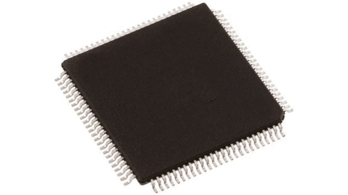
The image is for reference only, please refer to product details and specifications
Bulk discount available
Subtotal (1 unit)*
TWD357.00
(exc. GST)
TWD374.85
(inc. GST)
FREE delivery for orders over NT$1,300.00
Temporarily out of stock
- Shipping from August 13, 2026
Need more? Click ‘Check delivery dates’ to find extra stock and lead times.
Units | Per unit |
|---|---|
| 1 - 9 | TWD357.00 |
| 10 - 24 | TWD352.00 |
| 25 - 49 | TWD346.00 |
| 50 - 99 | TWD344.00 |
| 100 + | TWD336.00 |
*price indicative
- RS Stock No.:
- 772-0045
- Mfr. Part No.:
- iCE40HX1K-VQ100
- Manufacturer:
- Lattice Semiconductor
Specifications
Product overview and Technical data sheets
Legislation and Compliance
Product Details
Find similar products by selecting one or more attributes.
Select all | Attribute | Value |
|---|---|---|
| Brand | Lattice Semiconductor | |
| Product Type | FPGA | |
| Series | iCE40 | |
| Number of Logic Cells | 1280 | |
| Number of Logic Units | 160 | |
| Number of Registers | 1280 | |
| Mount Type | Surface | |
| Package Type | VQFP | |
| Minimum Supply Voltage | 1.14V | |
| Pin Count | 100 | |
| Maximum Supply Voltage | 1.26V | |
| Number of RAM Bits | 64000bit | |
| Minimum Operating Temperature | -40°C | |
| Maximum Operating Temperature | 85°C | |
| Standards/Approvals | No | |
| Height | 1.05mm | |
| Length | 14mm | |
| Automotive Standard | No | |
| Select all | ||
|---|---|---|
Brand Lattice Semiconductor | ||
Product Type FPGA | ||
Series iCE40 | ||
Number of Logic Cells 1280 | ||
Number of Logic Units 160 | ||
Number of Registers 1280 | ||
Mount Type Surface | ||
Package Type VQFP | ||
Minimum Supply Voltage 1.14V | ||
Pin Count 100 | ||
Maximum Supply Voltage 1.26V | ||
Number of RAM Bits 64000bit | ||
Minimum Operating Temperature -40°C | ||
Maximum Operating Temperature 85°C | ||
Standards/Approvals No | ||
Height 1.05mm | ||
Length 14mm | ||
Automotive Standard No | ||
Field Programmable Gate Arrays, Lattice Semiconductor
An FPGA is a semiconductor device consisting of a Matrix of Configurable Logic Blocks (CLBs) connected through programmable interconnects. The user determines these interconnections by programming SRAM. A CLB can be simple (AND, OR gates, etc) or complex (a Block of RAM). The FPGA allows changes to be MADE to a design even after the device is soldered into a PCB.